Tech
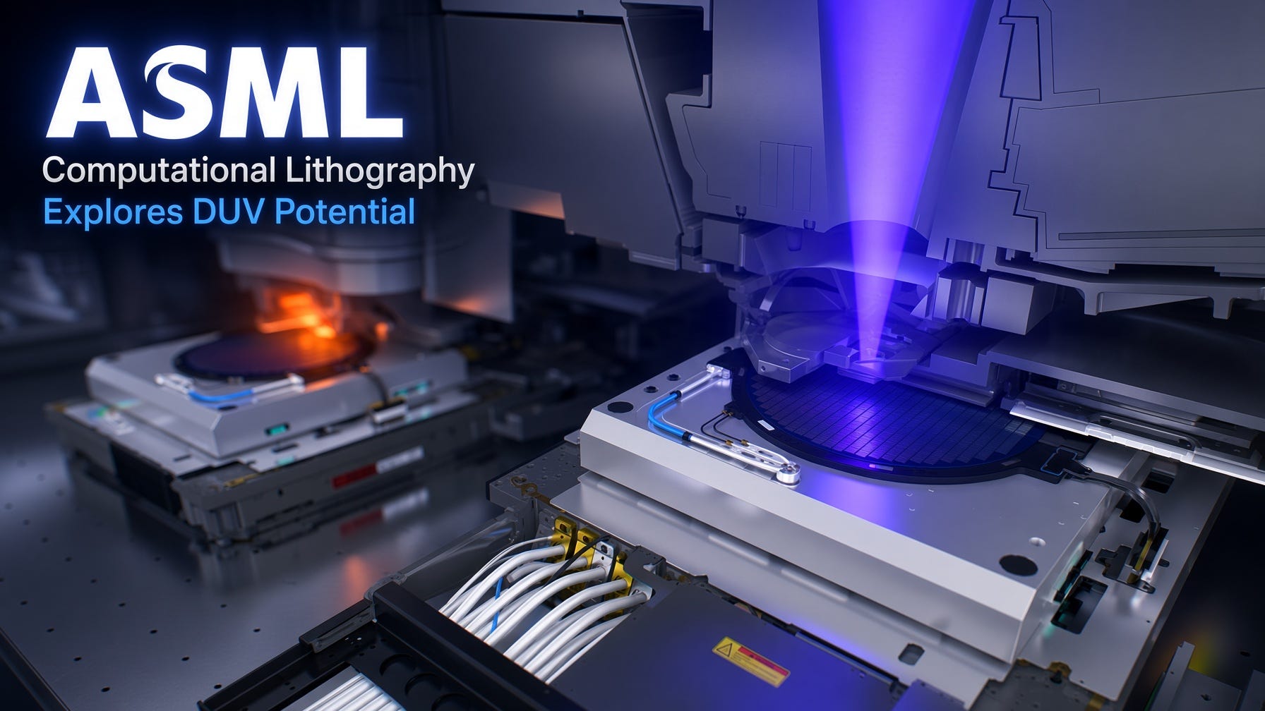
ASML Computational Lithography Explores DUV Potential
Meng Li · chippub
Sep 30, 2026 · 1 min listen · Last updated September 30, 2026
When the industry’s attention is fixed on EUV, an easily overlooked fact remains: the most numerous and highest-throughput lithography scanners in wafer fabs worldwide are still immersion DUV tools. 35 continue to expose a large share of critical layers in both advanced and mature processes, spanning advanced logic and memory manufacturing.
Listen · chippub
ASML Computational Lithography Explores DUV Potential
0:00-1:22
Pick your daily storyteller
Subscribe to match with Theo, Jessica, Chloe, Mason, Brock — your voice, every brief.
Live · Kokoro-82M