In AI data centers, thousands of chips must continuously exchange data. From inside the chip to between packages, and then between servers and racks, data transmission speeds keep rising, making interconnect technology a key industry focus.
Over the past few years, the industry has formed a relatively clear view: as transmission rates continue to increase, copper interconnects face growing pressure on bandwidth and power consumption. Optical interconnects are expected to become an important direction, and co-packaged optics (CPO) could further shorten the distance between optical components and chips.
However, outside this technology path, another technology that appears less eye-catching may be catching up quickly.
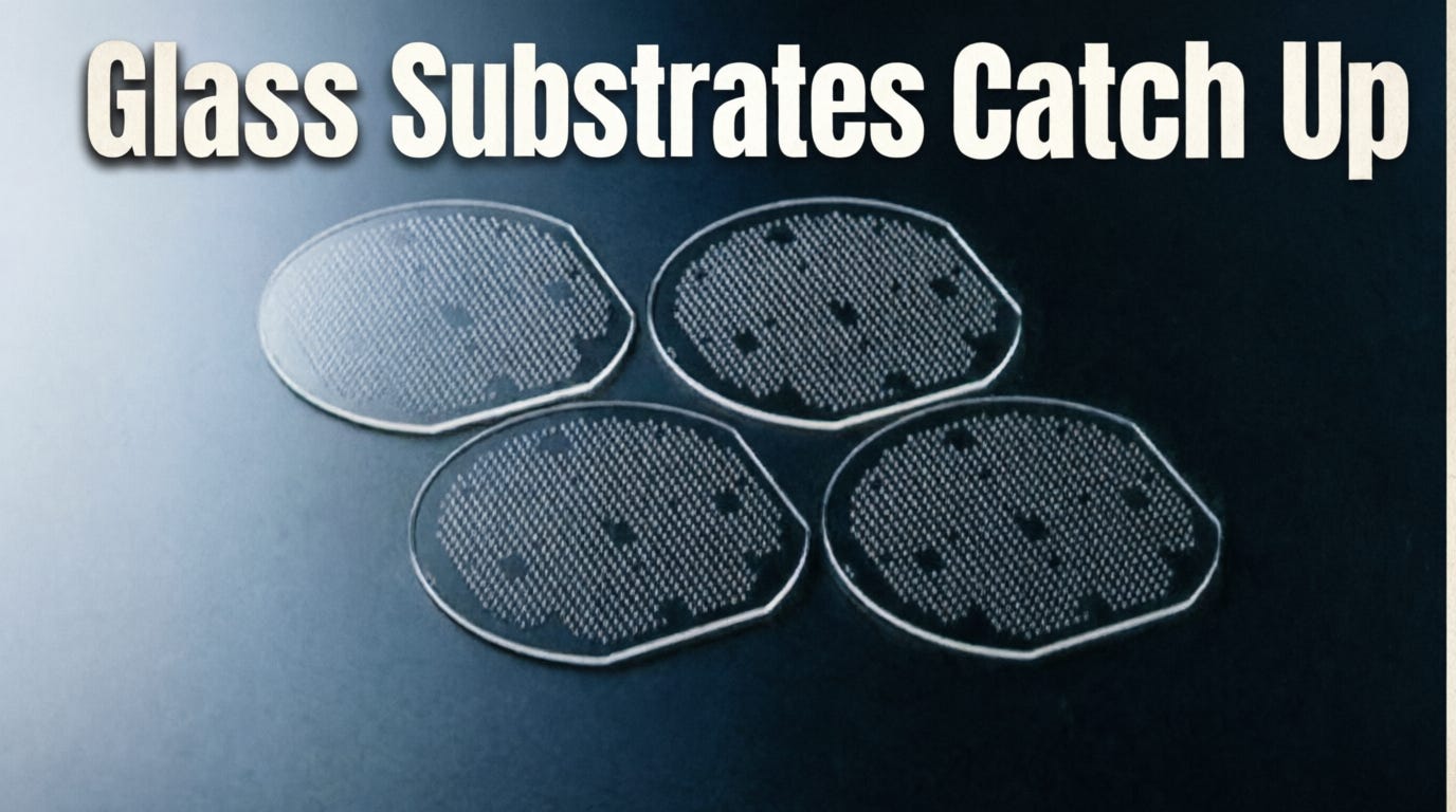
That technology is the glass substrate.
Compared with CPO, glass substrates have less technical buzz, but their industrialization tasks are relatively specific: how to create fine through-holes in glass, how to fill them with copper, how to control warpage of large-size substrates, and how to integrate these processes into a stable production flow.
If these problems can be gradually solved, glass substrates have a chance to enter next-generation AI chip packaging systems earlier. At least from the perspective of technical progress, they may achieve substantive breakthroughs sooner than CPO.