Tech
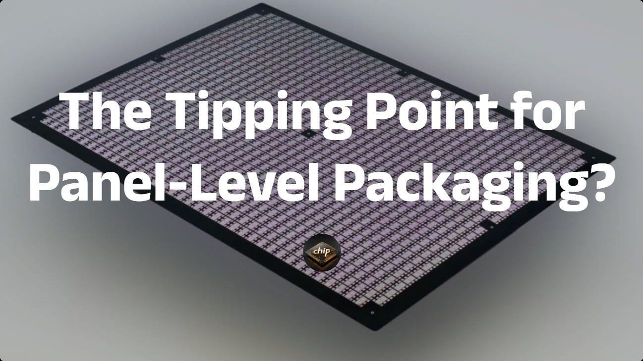
The Tipping Point for Panel-Level Packaging?
Meng Li · chippub
Oct 14, 2026 · 1 min listen · Last updated October 14, 2026
Advanced packaging technology is rapidly becoming a core driving force in the era of artificial intelligence and high-performance computing. This is largely due to the convergence of three major pillars: Panel-Level Packaging (PLP), back-end equipment innovation, and integrated circuit (IC) substrates.
Listen · chippub
The Tipping Point for Panel-Level Packaging?
0:00-0:58
Pick your daily storyteller
Subscribe to match with Theo, Jessica, Chloe, Mason, Brock — your voice, every brief.
Live · Kokoro-82M