Tech
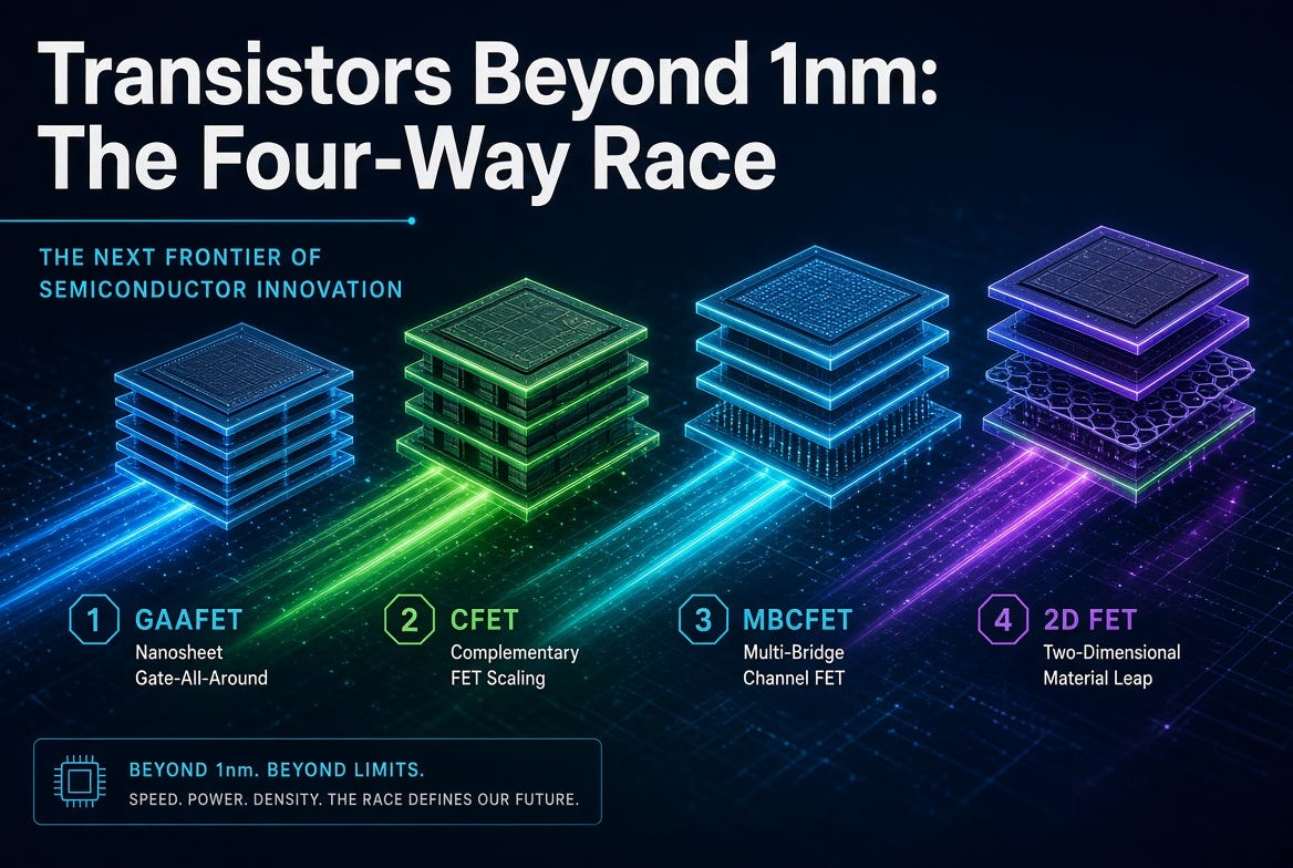
Transistors Beyond 1nm: The Four-Way Race
Meng Li · chippub
Oct 25, 2026 · 1 min listen · Last updated October 25, 2026
For two decades, the semiconductor industry has kept pace with Moore’s Law by repeatedly reshaping the transistor: from planar to FinFET, and now to the gate-all-around (GAA) nanosheet structure. Each generation has bought roughly another decade of scaling headroom.
Listen · chippub
Transistors Beyond 1nm: The Four-Way Race
0:00-0:52
Pick your daily storyteller
Subscribe to match with Theo, Jessica, Chloe, Mason, Brock — your voice, every brief.
Live · Kokoro-82M