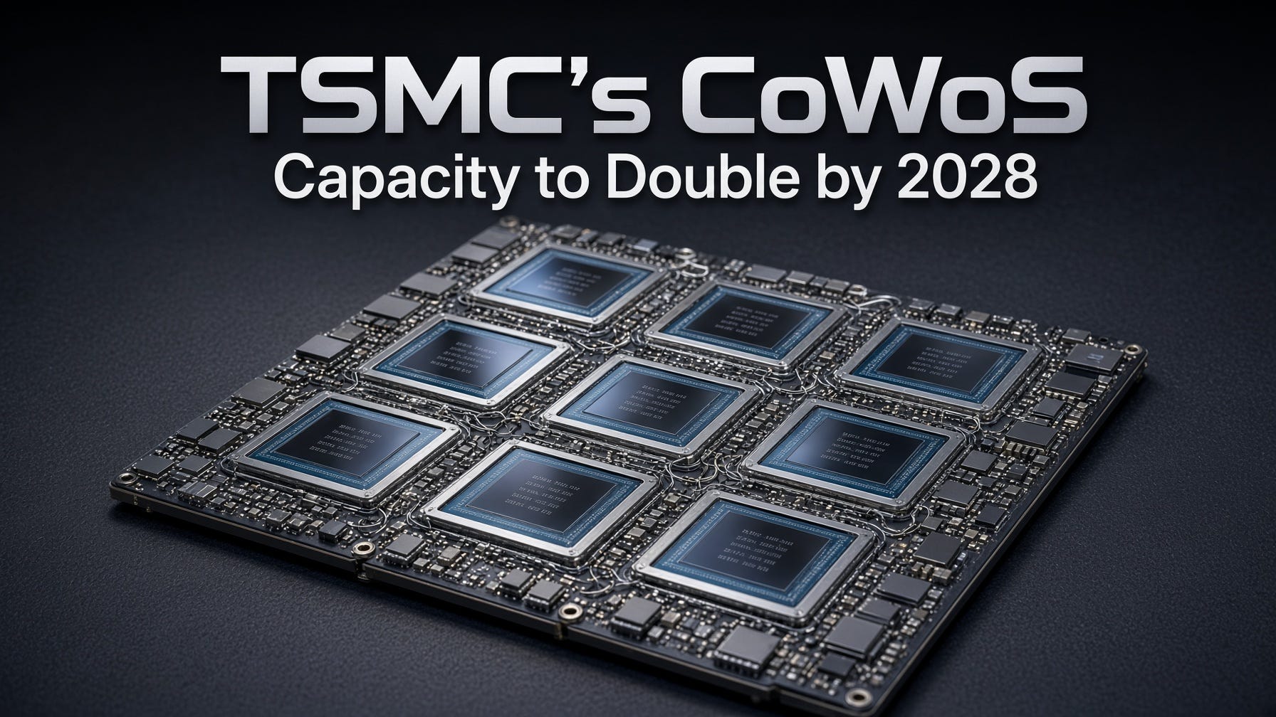
TSMC() plans to double its chip packaging (CoWoS) capacity by 2028 from 2026 levels. TSMC’s CoWoS is the leading packaging technology for AI GPUs and is widely adopted by major companies such as NVIDIA(****). Reports also note that this capacity expansion comes as existing capacity constraints have created spillover demand for other firms such as UMC and Amkor.
The report said Intel() is expected to reach CoWoS-equivalent wafer capacity of 45,000 wafers per month by 2028.
Strong demand for TSMC’s CoWoS technology and the resulting supply shortage have prompted other suppliers and technologies to emerge. Intel’s EMIB-T technology is one frequently mentioned in supply-chain reports. EMIB-T’s architecture is very different from CoWoS. It relies on pathways and circuits known as “bridges” embedded inside an organic substrate, with components such as logic chips and memory chips placed on top of those bridges.
CoWoS, by contrast, relies on an interposer to enable communication among memory chips, logic chips, and the host computer. That interposer consists of vertical circuits called through-silicon vias (TSVs). Their high-density design enables higher bandwidth and lower latency, which is well suited to high-performance AI chips from companies such as NVIDIA.
A Taiwanese media outlet, citing analysts, said TSMC() plans to raise CoWoS (wafer-level packaging) capacity to 260,000 wafers per month by the end of 2028, compared with an expected 130,000 wafers per month this year. The expansion will mainly be concentrated at TSMC’s Arizona fab in the United States and the AP7 plant in Taiwan. Although the Arizona fab can manufacture the latest chip products, because all of TSMC’s packaging capacity is in Taiwan, those chips must be air-shipped to Taiwan for packaging.