Tech
TSV, Too Hard
Meng Li · chippub
Oct 14, 2026 · 1 min listen · Last updated October 14, 2026
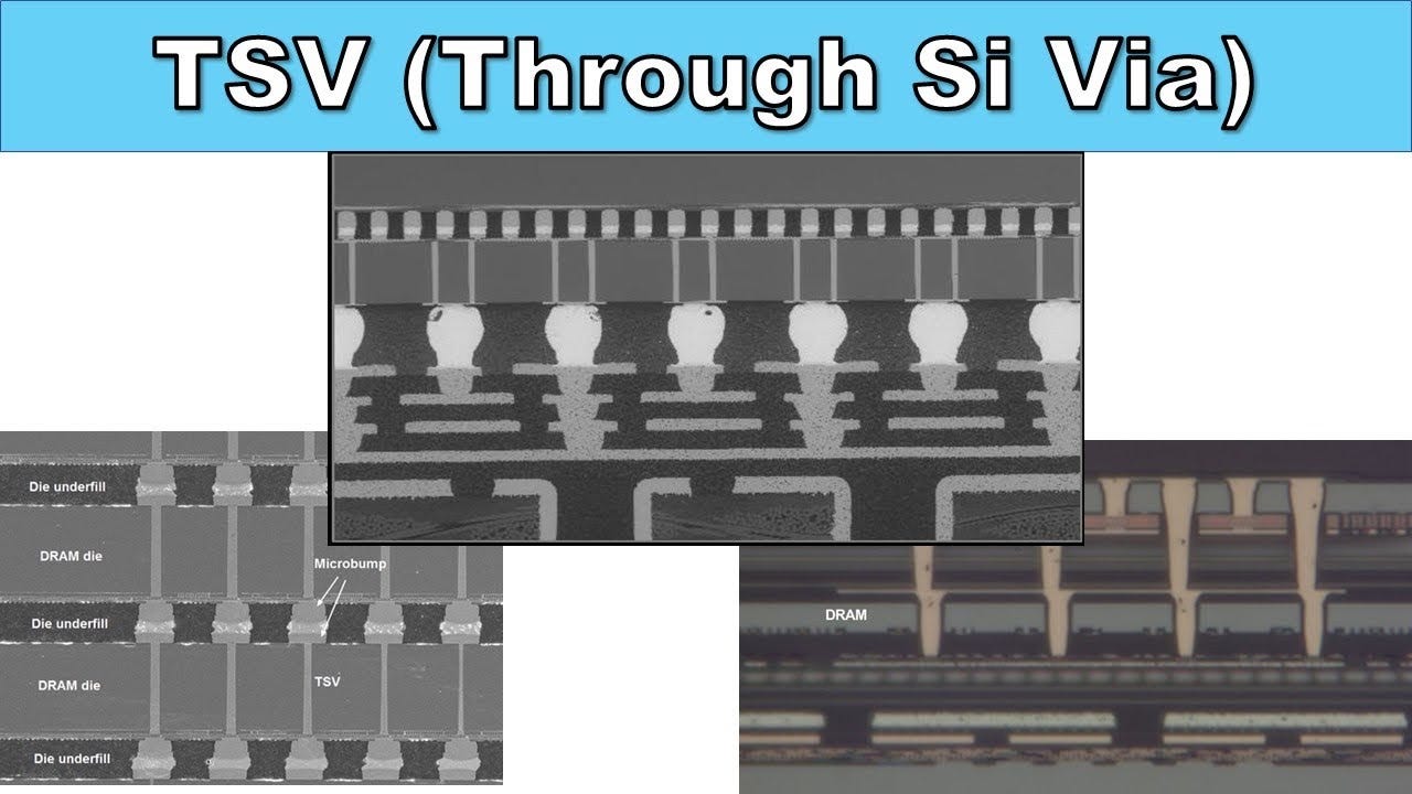
Through-Silicon Vias (TSV) provide the essential interconnects for high-bandwidth memory (HBM) stacking, silicon interposers, and emerging 3D chip stacking between DRAM chips. However, as TSV dimensions continue to shrink, their manufacturing cost becomes increasingly high, and the process is more prone to defects.
Listen · chippub
TSV, Too Hard
0:00-0:57
Pick your daily storyteller
Subscribe to match with Theo, Jessica, Chloe, Mason, Brock — your voice, every brief.
Live · Kokoro-82M